News
Superconductors and Light Will Transform AI
By Jeff Shainline · 22 May 2026
As featured in IEEE's The Bridge May 2026 Magazine "Super AI: The Interplay Between Artificial Intelligence and Superconductivity", https://hkn.ieee.org/wp-content/uploads/2026/05/Issue_2_2026.pdf
Abstract
Superconducting optoelectronic networks (SOEN) offer a new approach to artificial intelligence (AI). Conventional AI faces growing obstacles because its hardware and algorithms are poorly matched to the mechanisms of biological intelligence. Those mismatches drive high power consumption and make data-intensive tasks such as continuous video understanding far more difficult than they are for humans. SOENs combine superconducting computation with optical communication to implement neural systems more directly. This article examines the mismatch, explains how SOENs overcome it, outlines a path to scaling, and highlights near-term applications, along with the potential for economical, multi-generation growth.
1. Introduction
The release of ChatGPT-3 in late 2022 accelerated the long-running push toward powerful AI. Today’s leading systems are dominated by transformer-based large language models (LLMs) running on GPU (Graphics Processing Unit) hardware. This pairing has enabled chatbots, coding assistants, and many specialized models, but future scaling remains constrained by energy, latency, and cost. Inference is already expensive, and the capital and electricity required to train larger models are even more daunting. Latency also limits agentic workflows, in which autonomous systems must plan and act over many sequential steps. Transformer models have succeeded first in text because text is relatively compact. By contrast, systems that reason over sound and especially sight require much more data movement and memory. The longest context windows available in LLMs are in the order of a million tokens, only a few megabytes, whereas a ten-minute video contains vastly more information and therefore imposes immense computational demands. The fundamental challenge is not just computational throughput, but the ability to move and integrate vast amounts of data quickly and efficiently.
The architectural and algorithmic principles of the brain scale far better and learn far more efficiently than today’s dominant AI systems. Much more powerful AI should be possible with brain-inspired architectures, but existing hardware is poorly matched to the operations that support biological intelligence. Digital computing evolved to become general purpose and to perform complex mathematics with very small errors. Silicon transistors that encode information in binary form and execute Boolean logic are excellent for this task, yet the same devices and operations are not naturally suited to neural computation. To build significantly more powerful, efficient AI, we need hardware designed from first principles to implement neurons, synapses, dendrites, and their interconnections directly. The most effective route is to combine superconducting electronics for computation with integrated optics for communication at the single-photon level. This article explains why such a shift is necessary and what becomes possible if it succeeds.
2. Mismatch between today’s hardware and the operations of intelligence
Today’s AI is limited by a mismatch between available hardware and the operations known from neuroscience, to support deep intelligence. An intelligent system must build an internal model of the world and use that model to make decisions and guide actions. For a generally intelligentAI, that model must integrate not only text but also sound, sight, and other modalities. In both the brain and artificial systems, such representations emerge from synapses, dendrites, and neurons at the device level and from specialized processing regions that exchange information efficiently at the system level.
To build hardware for intelligence, the core computational primitives should be neurons, synapses, and dendrites themselves rather than digital approximations of what those elements do. These components should also be highly connected, so information can move easily among many processing regions. Analog implementations are attractive for two reasons. First, much of the information that intelligent systems must process is inherently analog. Speech varies continuously in amplitude and time; visual input varies across intensity, wavelength, space, and time; radar, RF signals, and many control signals are also analog. The simplest idea would be to operate silicon transistors as analog circuit elements, but that approach has serious drawbacks. In sub-threshold operation, MOSFET current depends exponentially on gate voltage, so small thresholdvoltage variations make large, interconnected analog transistor networks difficult to control.
Second, analog devices can be faster and more efficient for AI when they directly generate physical signals representing their inputs and outputs rather than forcing information into digital form. Across most computing, digital methods win because they are robust for arithmetic and logic. Neural computation is different: it depends on massive parallelism, redundancy, and rich interconnection. The brain shows that noisy analog primitives can nevertheless construct a distributed model of the world with unmatched efficiency for decision-making and action.
In neural networks, memory is crucial because it establishes synaptic weights, the factors that determine how strongly one neuron influences another. To instantiate those weights efficiently in hardware, memory elements should be distributed throughout the computational circuitry. Modern computing hardware separates processing and memory, creating the well-known Von Neumann bottleneck. If memory’s job is to store synaptic weights, the storage element should sit physically beside the synaptic circuit itself. Then, synaptic processing can occur without a separate call to a distant memory bank, and continuous learning through weight updates becomes natural. Co-locating memory and processing is difficult with current hardware, even though both rely on silicon transistors, because the process requirements for dense memory and fast logic differ.
Neural networks are also highly interconnected: a biological neuron typically makes thousands of connections, whereas a Boolean logic gate in a silicon processor rarely drives more than a few destinations. Resistive and capacitive parasitics on copper wiring make higher fan-out difficult. Light would be a natural communication medium for neural systems, but integrating efficient light sources with CMOS has been hard, and silicon photodetectors usually require many photons to register an event. A neuron that communicated optically on such a platform would therefore need a bright source to reach thousands of synapses. For these reasons, AI has generally adapted itself to available digital hardware rather than waiting for hardware better aligned with neural principles.
Superconducting optoelectronic networks are the way
These challenges can be overcome by combining superconducting electronics with optical communication at the single-photon level. We call these systems superconducting optoelectronic networks (SOENs) [1]. The key building blocks and architectural principles are summarized in Fig. 1
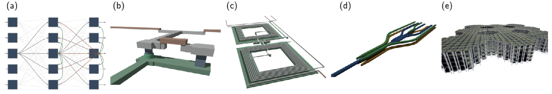
Superconducting electronic circuits are exceptionally wellsuited to analog information processing. The Josephson junction, a ubiquitous superconducting circuit element, can efficiently implement the operations of neurons, synapses, and dendrites [2,3]. Two Josephson junctions wired in parallel form a compartment that naturally sums many inputs. When coupled with an LR low-pass filter, this simple circuit can perform nonlinear transformations, including transfer functions widely used in modern AI, such as rectified linear, sigmoid-like, hyperbolic tangent, and quadratic responses. The same primitive can act as a synapse, dendrite, or neuron, depending on where it is placed in the circuit. Josephson junctions also provide the highest known speed-over-energy quotient of any circuit element, so no alternative is known that computes faster with less energy.
Superconducting circuits also solve the problem of colocating memory with processing. A simple circuit using four Josephson junctions can store high-bit-depth memory that interfaces directly with the synaptic circuit [4]. As information enters the synapse, it is multiplied by the locally stored synaptic weight, so memory access is not a separate operation. These memory cells are fabricated in the same process layers as the computational circuitry, can be programmed in a nanosecond, and can store anything from a single bit to roughly 12 bits—more than enough for current models, many of which are already moving toward four-bit precision or less. The weights can be programmed directly for supervised learning or modified by network activity for biologically inspired learning rules. Because the state is stored in a persistent superconducting current, it is non-volatile, and the state of every synapse can be read out and transferred to other systems.
Superconductors are excellent for analog processing and integrated memory, while light is ideal for communication because it avoids wiring parasitics and supports extreme fan-out. SOENs therefore use superconducting singlephoton detectors, simple superconducting wires that can be patterned with a single lithography step, exhibit high yield, and interface seamlessly with Josephson junctions [5]. These detectors are fast enough for neurons to send and receive communication events up to 100 MHz, roughly a million times faster than biological neurons. Although 100 MHz sounds slow compared with a multi-gigahertz processor clock, each neuron can deliver approximately 8-bit signals to more than 1,000 destinations, corresponding to aggregate communication near 800 Gbps.
This architecture reaches two crucial physical limits of intelligence: light-speed communication across very large networks and signaling at the single-photon level. The same communication format scales from on-chip nanophotonic waveguides to long-range fiber links. Each neuron has direct, dedicated connections rather than contending for a shared address space, so activity elsewhere in the network does not create traffic-dependent bottlenecks, and latency is fundamentally set by the speed of light.
With this approach, both active circuits and passive wiring and waveguides can be fabricated at a wafer scale in multiple planes of the same wafer. Superconducting circuits are larger than semiconductor transistors, but multiple layers of Josephson junctions and single-photon detectors can be produced with conventional deposition, lithographic patterning, etching, and planarization, increasing circuit density. Their low power dissipation allows heat extraction by thermal conduction to a surrounding liquid-helium bath. Performance does not improve indefinitely by shrinking these devices below a certain scale, so fabrication can rely on mature, lower-cost foundries rather than the most advanced CMOS nodes. That lowers wafer cost dramatically and broadens manufacturing options geographically.
Does cryogenic cooling make this approach impractical? No. This hardware operates at 4 kelvins, about 100 times warmer than superconducting quantum computers that require millikelvin temperatures. It therefore needs only ordinary helium-4 rather than the expensive helium-3 mixtures used in dilution refrigerators. Closed-cycle helium refrigerators capable of cooling systems with 10 trillion parameters are available today. Their purchase price is roughly $6M, about 20% of the capital equipment cost of such a system, and because they operate in a closed cycle, the helium inventory—around $55,000 worth—does not need continual replenishment.
Some may argue that conventional chips or incremental augmentations to current roadmaps will overcome AI scaling limits. GPUs have improved across recent generations, but mainly by consuming more energy, especially for training. The superconducting optoelectronic approach can increase performance by orders of magnitude and reduce energy consumption by orders of magnitude relative to current practice. More focused improvements, such as inference accelerators or optical interconnects, help only modestly if the underlying mismatch between the hardware substrate and the operations of intelligence remains unresolved.
3. The Roadmap
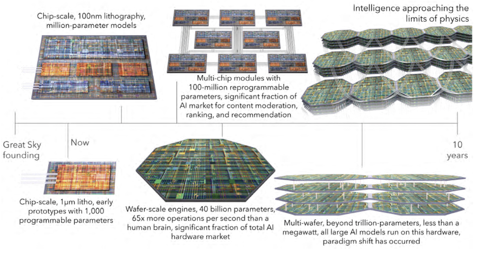
The roadmap for developing this technology is shown inFig. 2. In the past year, we taped out three wafers. The first achieved image classification of small images at up to 10 million frames per second. The second focused on speech processing and demonstrated classification of more than a million spoken words per minute. The third is a reprogrammable chip with 1,008 configurable parameters that can execute many networks across application spaces.
Going forward, the primary objective is to scale. With lithography capable of 100 nm features, parameter density can increase by more than two orders of magnitude. Interconnecting many die in multi-chip modules (MCMs) opens important commercial applications. At that scale, achievable in roughly three years, we can construct models with about 100 million reconfigurable parameters. Such networks can address workloads, including video analysis and signal processing, and, at this model size, substantial revenue becomes possible.
A further step of change in performance and market applicability comes with wafer-scale modules. A single 300 mm wafer can support roughly 40 billion parameters with continuous learning. Such a wafer would perform about 65 times more operations per second than a human brain and provide 4,300 times the bisection bandwidth of a state-of-the-art GPU system. The SOEN neural architecture enables deeply intelligent models, and this immense communication bandwidth supports the data movement required to integrate information efficiently across the network. This is the scale at which the architecture’s communication advantages become especially important.
To reach trillion-parameter models, multiple wafers can be densely integrated, using free-space optical communication to couple transmitters on one wafer to single-photon receivers on vertically stacked wafers. Fiber optics handle longer distances. SOEN systems can therefore scale across many product generations, not by shrinking features in the manner of Moore’s law, but by integrating ever larger computational resources into one coherent cognitive system. Exponential growth becomes possible because of the low power density of superconducting circuits, the integration of processing and memory, photonic communication across very large systems, and comparatively low manufacturing costs. Physics thus enables economically viable, transformative technology.
4. Comparing to current practice
Implementing neural networks with superconductors and light goes beyond incremental improvement; it changes the cost-performance curve for AI. The platform can help close the gap between today’s enormous capital spending on AI infrastructure and the revenue those systems generate. For current LLM workloads, the reduced capital cost, higher throughput, and better energy efficiency of SOENs are projected to yield roughly 300 times lower cost per token than leading GPUs through 2027.
The advantage grows with system scale and data throughput. For a trillion-parameter video-analysis model, the cost per inference could drop by more than six orders of magnitude. Such savings arise because video is data-intensive and transformer architectures are poorly matched to it. Leading video-comprehension transformers often process about one frame per second, whereas a superconducting optoelectronic network can analyze the order of 60 million frames per second, independent of frame size and video duration. A megapixel array of optical transmitters can project through a window to a single-photon-sensitive artificial retina inside the cryostat, delivering about 3 Pbps into the neural model. Lower system power combined with far higher throughput drives energy savings.
5. Future Possibilities
This technology opens many market opportunities. As an entry point, rapid video analysis is feasible within a few years. Every video uploaded to a social media platform is analyzed by several models for several purposes, and many of those models contain between one million and one hundred million parameters—a range SOENs should reach in two to three years. The high speed of the hardware offers major advantages in latency and throughput, enabling lower-cost, lowerpower systems that can guarantee response times far below what is currently practical, even during heavy traffic. As online platforms become increasingly burdened by AI-generated content and automated traffic, demand for rapid and accurate analysis will continue to grow. At similar scales, deep-learning recommendation models become attractive targets as well. These are real commercial workloads rather than speculative demonstrations.
By first addressing rapid-analysis use cases with lightweight models, the platform can prove its performance while building market trust. As networks scale, the addressable markets expand. Universal assistants that hear what users say and see what they see through phones, glasses, or other wearables are highly sought after, but today’s multimodal models remain expensive in terms of hardware and power. Leading systems that fuse audio and video with long context may process only a single video frame per second, making wide deployment difficult. A trillionparameter SOEN model with multimodal intelligence and lifelong learning is projected to cost about $30M and could sustain continuous conversations with a million people simultaneously with no perceptible latency.
Video analysis and universal assistants are only early examples of a broader technological shift. Other promising applications include high-speed control of robotic fleets and fusion reactors [6], biological and medical systems, constrained optimization, cybersecurity, and quantumneural hybrid systems. We have shown that the technology is possible; the next step is to scale it until it becomes broadly useful.
References:
[1] Jeffrey M Shainline. Optoelectronic intelligence. Applied Physics Letters, 118(16):160501, 2021.
[2] Patrick Crotty, Dan Schult, and Ken Segall. Josephson junction simulation of neurons. Physical Review E, 82(1):011914, 2010.
[3] Jeffrey M Shainline, Sonia M Buckley, Adam N McCaughan, Jeffrey T Chiles, Amir Jafari Salim, Manuel Castellanos-Beltran, Christine A Donnelly, Michael L Schneider, Richard P Mirin, and Sae Woo Nam. Superconducting optoelectronic loop neurons. Journal of Applied Physics, 126(4), 2019.
[4] Bryce A Primavera, Saeed Khan, Richard P Mirin, Sae Woo Nam, and Jeffrey M Shainline. Programmable superconducting optoelectronic single-photon synapses with integrated multi-state memory. APL Machine Learning, 2(2), 2024.
[5] Saeed Khan, Bryce A Primavera, Jeff Chiles, Adam N McCaughan, Sonia M Buckley, Alexander N Tait, Adriana Lita, John Biesecker, Anna Fox, David Olaya, et al. Superconducting optoelectronic single-photon synapses. Nature Electronics, 5:650–659, 2022.
[6] Jonas Degrave, Federico Felici, Jonas Buchli, Michael Neunert, Brendan Tracey, Francesco Carpanese, Timo Ewalds, Roland Hafner, Abbas Abdolmaleki, Diego de Las Casas, et al. Magnetic control of tokamak plasmas through deep reinforcement learning. Nature, 602(7897):414–419, 2022.